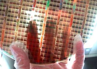
A “thinned” wafer ready to be joined to another
IBM said on Wednesday it will be able to make microchips faster and more energy efficient by stacking components on top of each other, a breakthrough that cuts the distance an electrical signal needs to travel.
The technique works by drilling tiny holes through a wafer of silicon and filling them with metal. Components such as memory can then be stacked on top of the main part of the chip, eliminating the need for wires stretching out to the sides.
IBM likened the method to replacing a sprawling airport parking lot with a multi-storied garage right next to the terminal. Like people walking from the garage to the terminal, electrical signals do not have to travel as far in a chip with stacked components.
IBM will use the method to make power management chips for wireless devices later this year, allowing them to use 40 percent less power than previous versions, Lisa Su said in an interview.
They plan to follow-on with processors for larger devices. An obvious example why a solid program of R&D keeps the best tech companies in business seemingly forever.
More on the technology over here.


Very cool but also very Seymour Cray.He developed some ground breaking tech that had more to do with design than technological inovation.Kudos to IBM.
Stacking parts in chips is a breakthrough? Umm, no, that isn’t a leap of the imagination at all, it’s a parallel idea based on current multi-layer IC design.
OTOH, I didn’t see anything in the article about cooling said components.
This was bound to happen as we are nearing the limit of shrinking the circuitry. Nowhere left to go but up.
Clicking the second link – “here” – at the bottom of the Post leads you to more of the decade-plus history of this project.
IBM develops breakthrough technology only to let it marinate in their patent drawers and then milk other companies for license fees.
#5 – Angel, you may be right as usual; I don’t know. But if IBM does that, it’s another compelling argument in favor of a “use it or lose it” provision in patent and copyright laws.
Yep, and I would Love to see a 5 year, release of Software…
Any software made would be released to open market, and FREE, after 5 years.. Including Source.
thats how the market is running, why not Force it to Keep improving.
#6 & #7
I agree with you both 100% on this.
I just wish IBM’s execs and corporate lawyers could see beyond the year’s 4 Quarter earnings report…
Here too, heat still is going to be a limiting parameter.
It will be interesting if they finagled better ways to extract heat from the stack layers or instead use low power chips to reduce the heat generated, or both methods.
Will packaging cost outweigh consumer demand for ever cheaper and powerful computers.
Stay tuned, same bat channel, same bat time. Not a done deal in the market yet.
HAH!
Chip stacking technique, how original!
This reminds me of the days when I used to put my TV on one side of the room, and my VHS VCR on the other side of the room. Then one day, after I got sick of tripping on the cords, I thought, “Hey, I could put the VHS VCR on the same stand as the TV. Wow, how incredibly friggin’ revolutionary. The thought was so amazing, I thought about patenting the idea. However, I didn’t patent it — it seemed obvious after a little consideration. Kind of like Vonage versus Roger Wilco.
To think, IBM could be working for me now because of patent issues…
10,
This reminds me of the Layer’d mobo…WHICH they use in most laptops for the last 15 years…
The only diff, is that these are ALOT thinner.